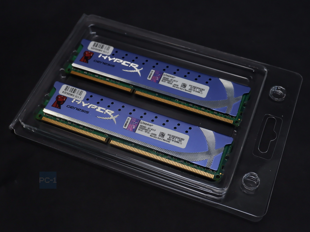
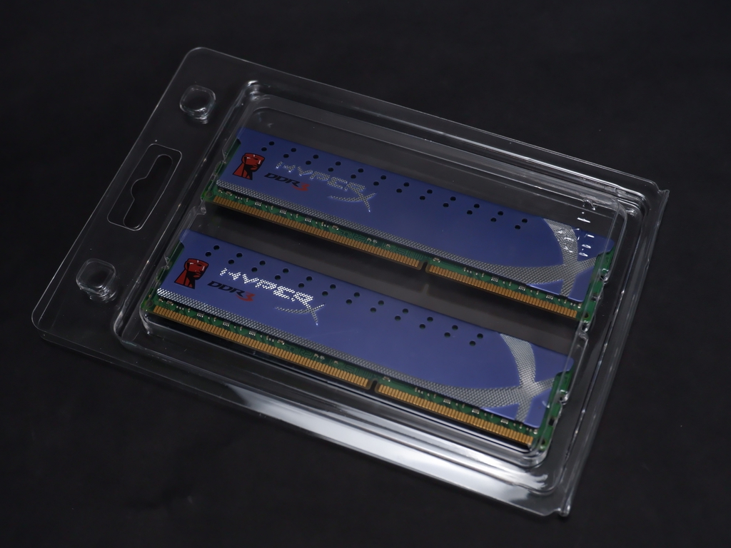
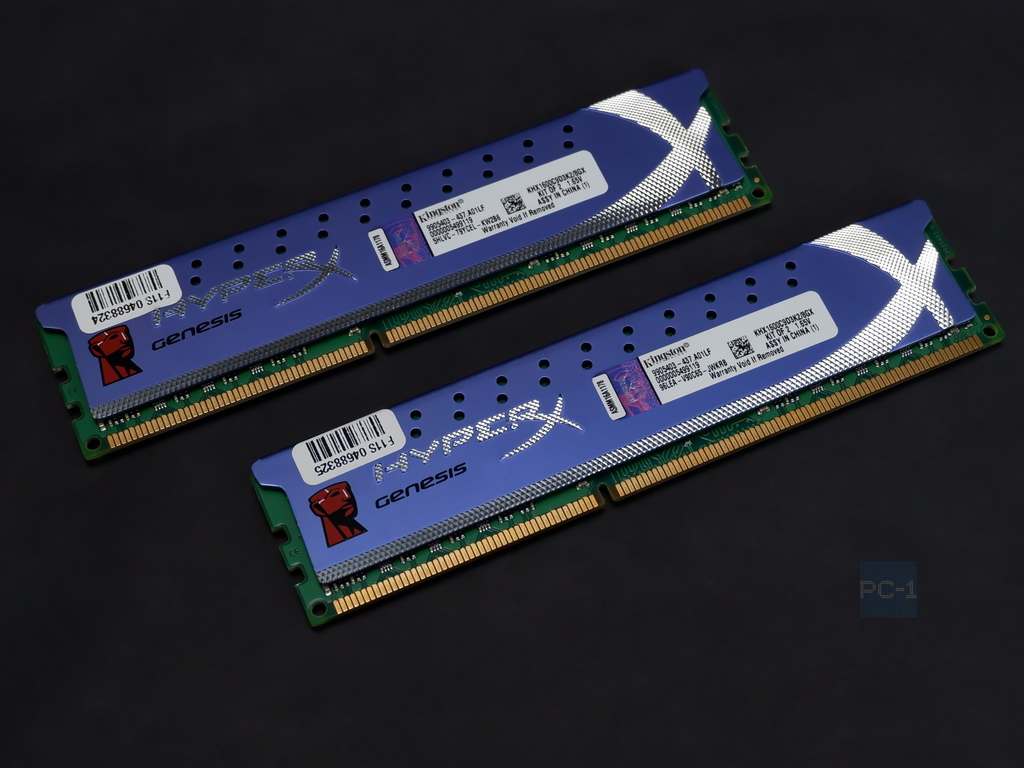
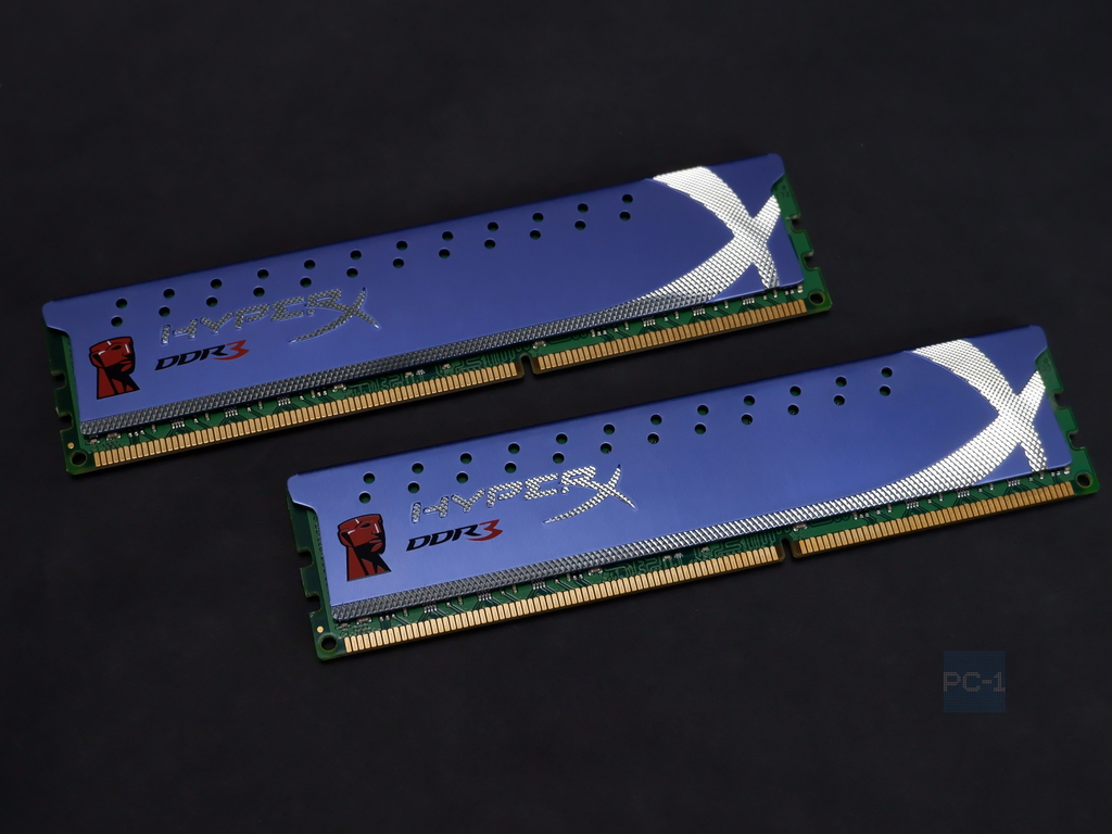
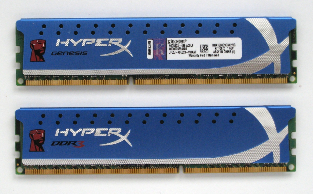
Парные Модули памяти DDR3 8Gb KIT (2x4Gb) Kingston Hyper Genesis KHX1600C9D3K2/8GX 1600 CL9 240-Pin DIMM Kit (4GB 512M x 64-Bit x 2 pcs.)
Два модуля по 4 Гб x 2 шт. ✔DDR3 ✔PC3-12800 (DDR3 1600 МГц) ✔до 1600 МГц ✔Поддержка XMP (Intel Extreme Memory Profiles) ✔Радиатор
Комплект из 2х модулей памяти для использования с процессорами Core i7 (также совместимо с AMD)
Частота функционирования до 1600 МГц
Стандарт памяти PC3-12800 (DDR3 1600 МГц)
Пропускная способность: 12800 Мб/с
Латентность: CL9
Тайминги: 9-9-9
Напряжение питания: 1.65 В (Напряжение памяти нестандартное — выставляется в БИОС вручную)
Парные Модули памяти Kingston HyperX KHX1600C9D3K2/8GX DDR3 2x4 Гб <pc3-12800>
SPECIFICATIONS Power will vary depending on the SDRAM used. KHX1600C9D3K2/8GX 8GB (4GB 512M x 64-Bit x 2 pcs.)
DDR3-1600 CL9 240-Pin DIMM Kit Continued
FEATURES Kingston's KHX1600C9D3K2/8GX is a kit of two 512M x 64-bit (4GB) DDR3-1600 CL9 SDRAM (Synchronous DRAM) 1Rx8 memory modules, based on eight 512M x 8-bit DDR3 FBGA components per module. Each module kit supports Intel® XMP (Extreme Memory Profiles). Total kit capacity is 8GB. Each module kit has been tested to run at DDR3-1600 at a low latency timing of 9-9-9-27 at 1.65V.
The SPDs are programmed to JEDEC standard latency DDR3-1600 timing of 11-11-11 at 1.5V. Each 240-pin DIMM uses gold contact fingers and requires +1.5V. The JEDEC standard electrical and mechanical specifications are as follows: •
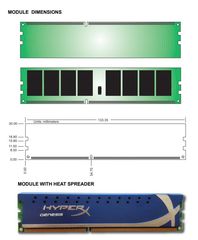
JEDEC standard 1.5V (1.425V ~ 1.575V) Power Supply • VDDQ = 1.5V (1.425V ~ 1.575V) • 800MHz fCK for 1600Mb/sec/pin • 8 independent internal banks • Programmable CAS latency: 11, 10, 9, 8, 7, 6 • Programmable Additive Latency: 0, CL — 2, or CL — 1 clock • 8-bit pre-fetch • Burst Length: 8 (interleave without any limit, sequential with starting address “000” only), 4 with tCCD = 4 which does not allow seamless read or write (either on the fly using A12 or MRS) • Bi-directional Differential Data Strobe • Internal (self) calibration: Internal self calibration through ZQ pin (RZQ: 240 ohm ± 1%) • On Die Termination using ODT pin • Average Refresh Period 7.8us at lower than TCASE 85°C, 3.9us at 85°C < TCASE < 95°Cº • Asynchronous Reset • PCB: Height 1.180” (30.00mm), single sided component